After announcing an approximately $25 billion investment into semiconductors and display technology in 2016, Samsung is showing off some of the results of that cash injection.
The company has announced its fourth-generation 14-nanometer (nm) process and third-generation 10nm process to be implemented in next-generation products across both their mobile and consumer electronics product lines, as well as in data centre and automotive solutions.
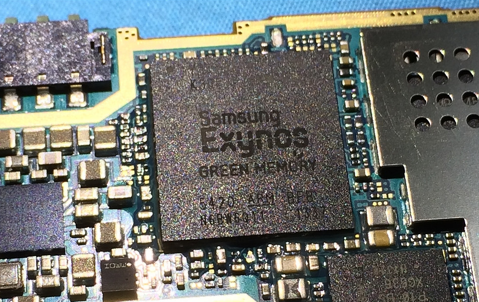
For those unfamiliar with the terms used above, the two processes will be used in semiconductor device fabrication to create new 14nm and 10nm Systems-on-a-Chip (SoC). The 14nm chip was first commercially shipped by Intel in 2014, while Samsung started mass production on mobile processors that feature 10nm FinFET technology this year. Rumours have the technology potentially debuting in Qualcomm’s Snapdragon 830, and it could also be used in Samsung’s own 2017 flagship Exynos SoC.
The company states that its new 14nm process technology delivers improved performance at the same power and according tot the same design rules compared to its previous 14nm process.
Meanwhile, the new 10nm process technology will provide area reduction compared to its previous generations. Samsung says it’s expected to be “the most cost-effective cutting-edge process technology in the industry.”
The South Korean tech giant also updated 7nm Extreme Ultraviolet Lithography (EUV) process development status and showcased its 7nm EUV wafer, which is generally expected to hit the market in 2019.
Samsung states process design kits for the new technologies will be available in the second quarter of 2017, meaning the resulting new chips may become commercially available in 2018.
Image credit: Honou
Related: Samsung starts production on 10nm FinFET mobile processors
[source]Samsung[/source][via]Android Authority[/via]
MobileSyrup may earn a commission from purchases made via our links, which helps fund the journalism we provide free on our website. These links do not influence our editorial content. Support us here.